April 2021
This project details the process of creating prototype PCBs using a home CNC machine. Mastering this skill requires significant time investment—approximately 3-4 weeks of focused effort—though subsequent projects become faster once proficiency is achieved.
The Workflow
The process consists of these main steps:
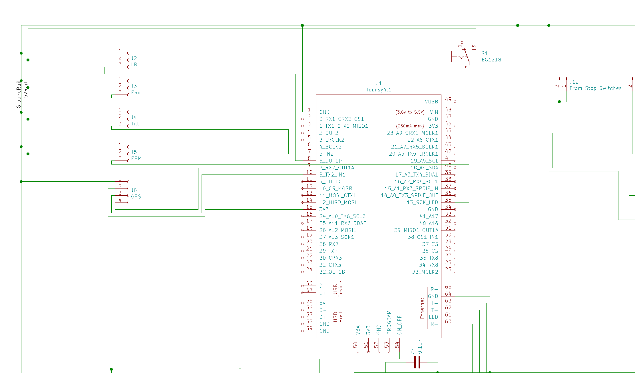
- Create circuit schematic (using KiCad)
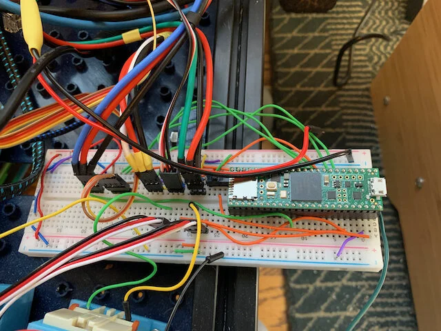
- Test design on breadboard
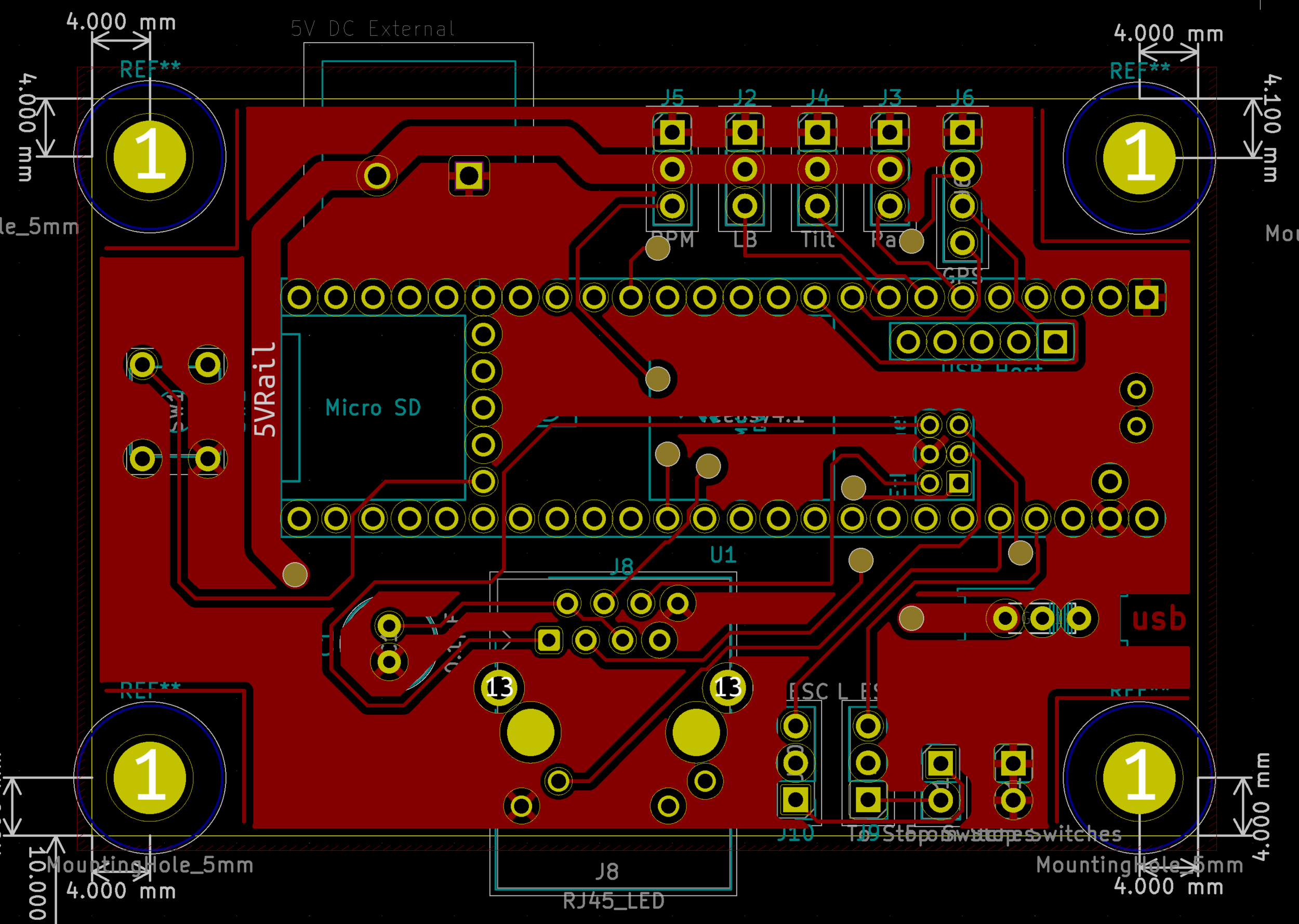
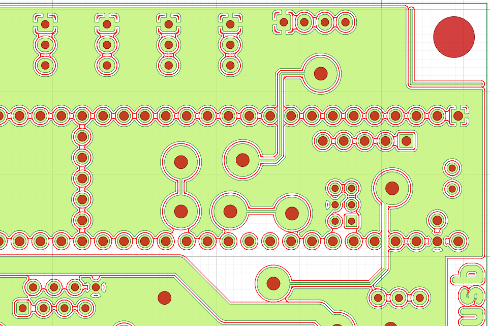
- Create board layout in KiCad
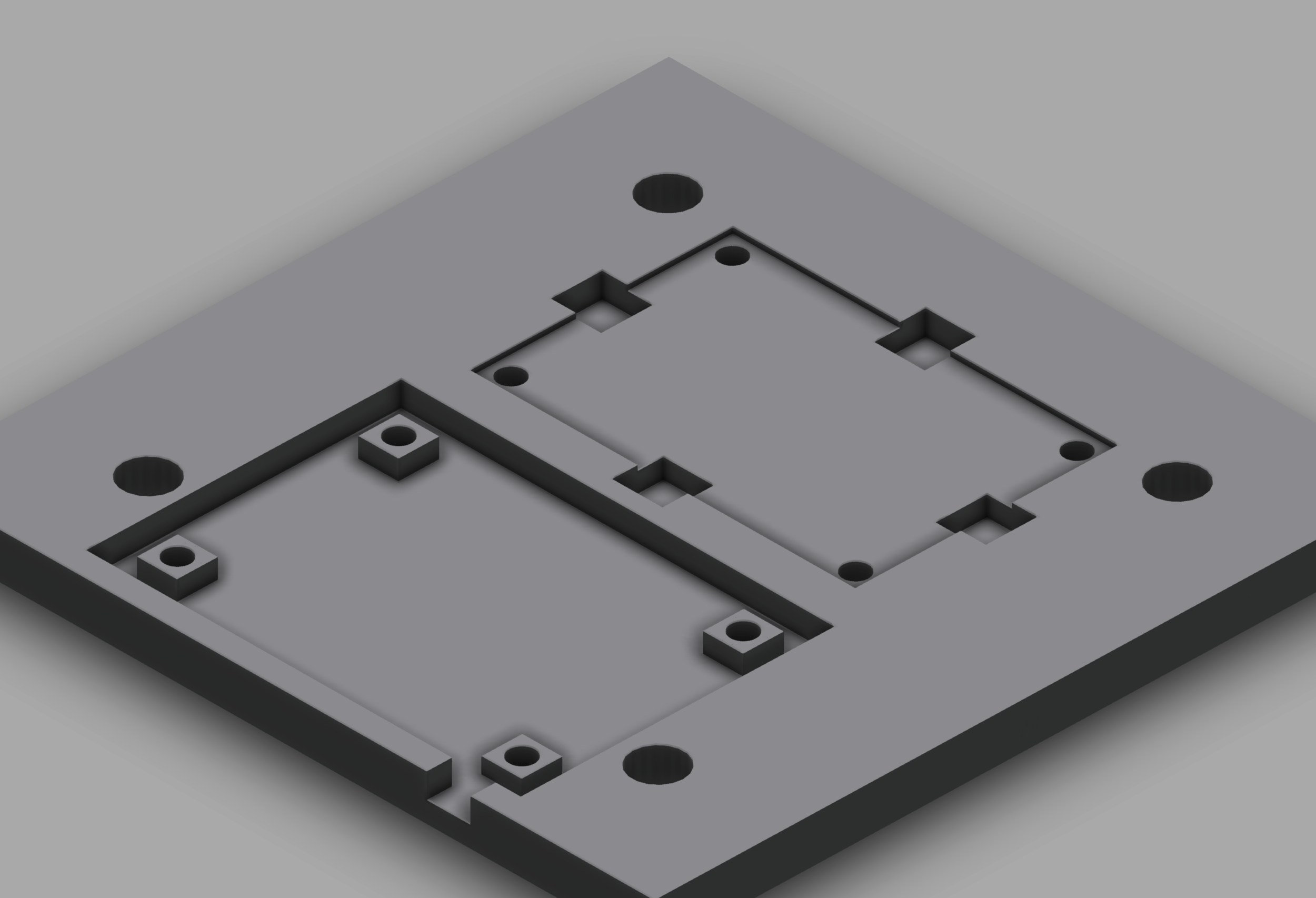
- Make a jig for double-sided milling
- Prepare G-code files
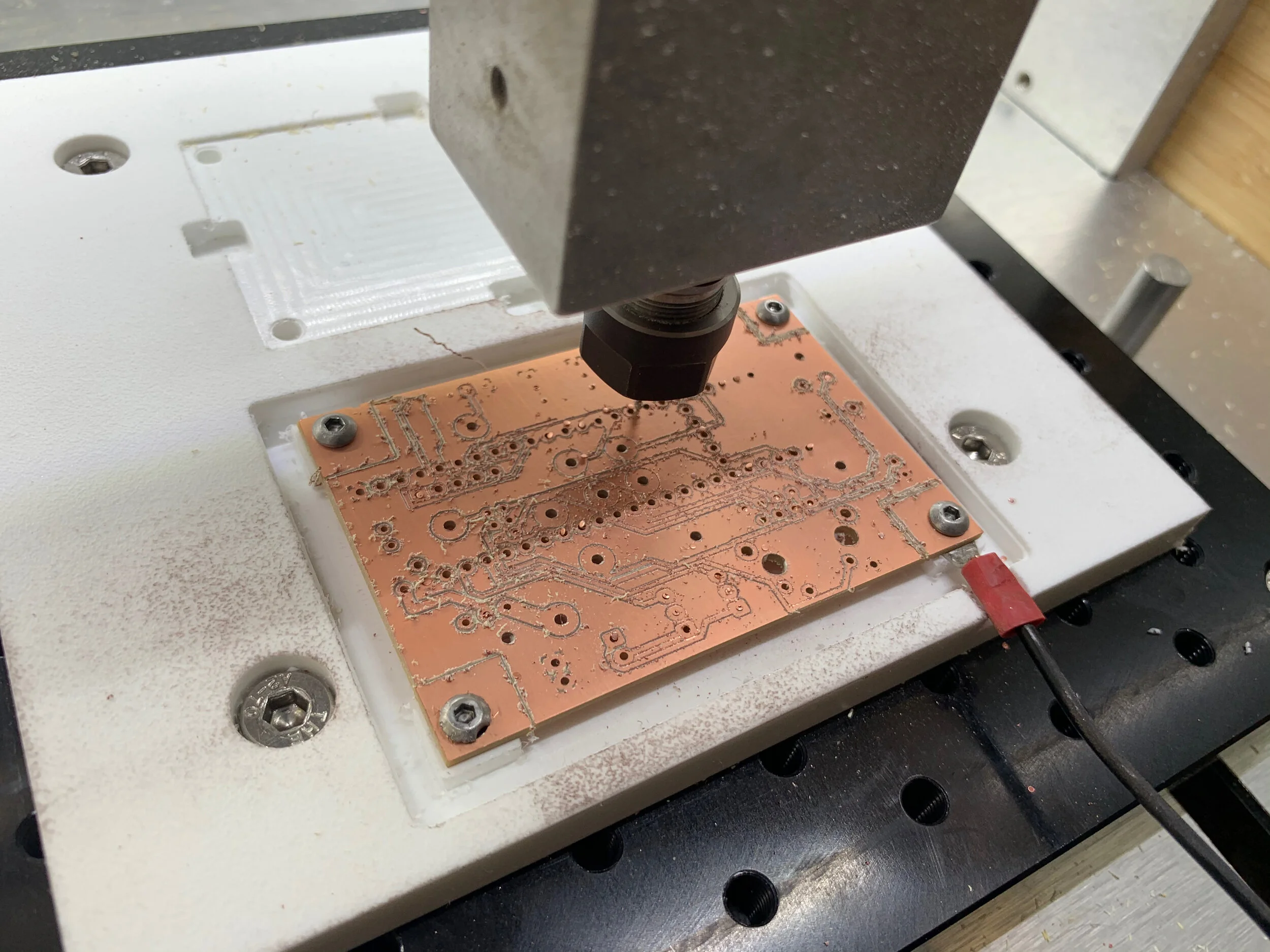
- Mill and drill the PCB
Hardware
- Carbide 3D Nomad 3 CNC machine
- 3/8" HDPE stock for jig material
- FR1 copper clad blanks (2"×3" double-sided)
- BitZero2 probe
- 1mm carbide drill bits
- Fine-tipped carbide scribe for scratch milling
- M3 rivet nuts for PCB mounting
Software Tools
KiCad
Open source PCB design software for creating schematics and board layouts.
FlatCam
Converts Gerber and Excellon files to G-code. Version 8.993 Beta recommended for usability. Windows installation most reliable.
bCNC
Alternative CNC controller with auto-leveling capabilities. Performs better on Windows/Linux than macOS. Steeper learning curve than Carbide Motion.
KiCad Board Layout Tips
- Set trace clearance to 0.34mm for tight routing
- Plan which side will be soldered (design accordingly)
- Use Edge.Cuts layer for PCB borders
- Trace power lines first, then signals, then ground fills
- Create fence traces around mounting holes to prevent bit collisions
- Use tiny M3 screws/nuts as vias (4mm via size, 1.6mm drill)
- Select breadboard-compatible components (2.54mm pitch)
FlatCam Parameters for Scratch Milling
- Tool diameter: 0.5mm
- Cut depth (Z): -0.35mm
- Travel height: 3mm
- Feed rate X-Y: 2500mm/min
- Spindle speed: 0 (passive scratch method)
Key Takeaways
- Home PCB milling is viable but requires mastery of multiple software tools
- Scratch milling (rather than full isolation routing) produces faster results
- Precise jig design is critical for double-sided alignment
- Auto-leveling compensates for uneven copper clad surfaces
- One-time projects may be better served by commercial PCB manufacturers
Resources